The Group
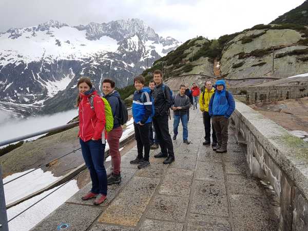
Members of our group together with the Eduphys Group or Prof. Dr. Andreas Vaterlaus at Gelmersee (2019).
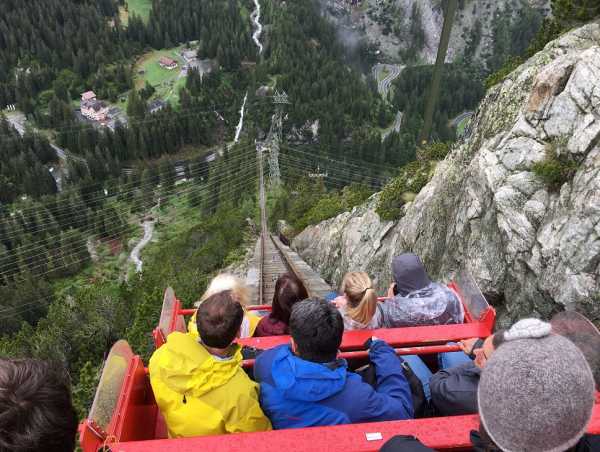
 Members of our group together with the Eduphys Group of Prof. Dr. Andreas Vaterlaus in the Gelmerbahn (2019).
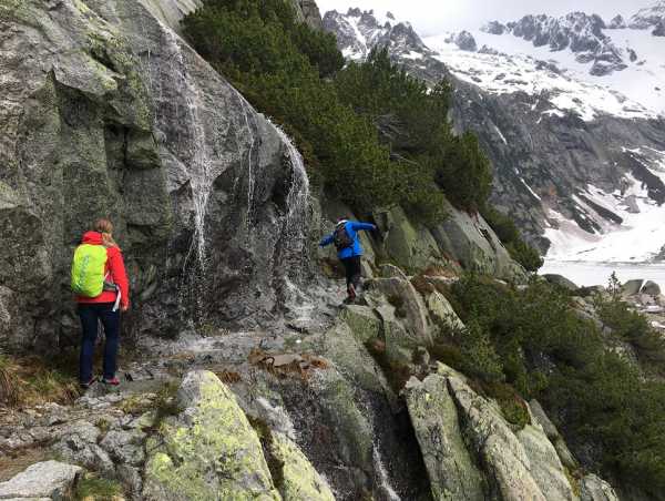 Hiking at Gelmersee (2019)
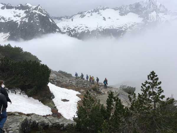 Members of our group and the Eduphys group of Prof. Dr. Andreas Vaterlaus in the Grimselwerk (2019).
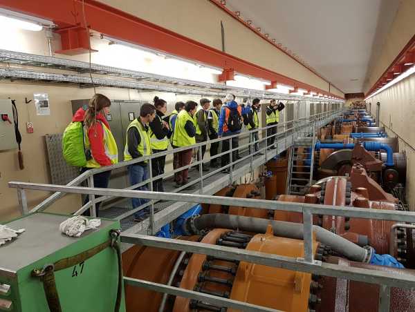 Group Excursion in 2018 to Bergell together with the Eduphys group of Prof. Dr. Andreas Vaterlaus.
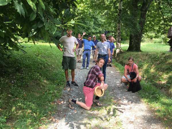 Group Excursion together with Eduphys Group.
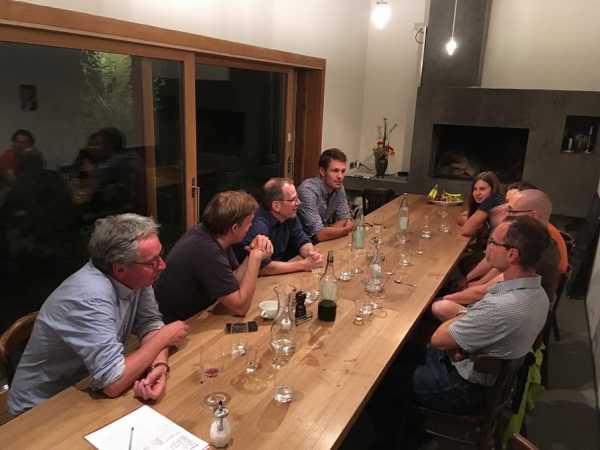
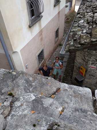 Group excursion to Brienzer Horn, Microphys and Eduphys Group (2015).
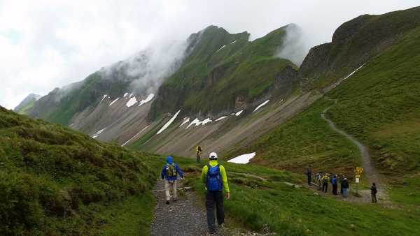 Los Magnetostaticos at Boltzmann Cup (2013).
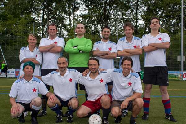 Group excursion to Breda, Microphys and Eduphys Group (2011).
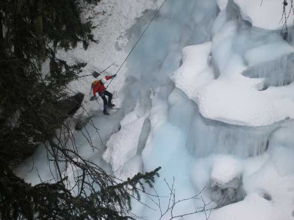
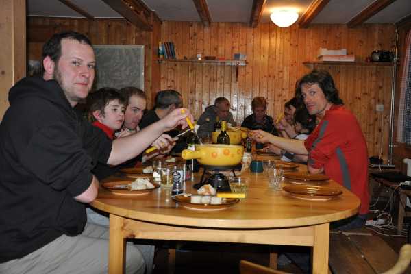 Ice Climbing in Breda (2011).
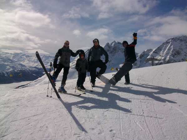
 Skiing in Breda (2011)
 Members of our group together with the Eduphys Group of Prof. Dr. Andreas Vaterlaus in the Gelmerbahn (2019).

 Hiking at Gelmersee (2019)
 Members of our group and the Eduphys group of Prof. Dr. Andreas Vaterlaus in the Grimselwerk (2019).
 Group Excursion in 2018 to Bergell together with the Eduphys group of Prof. Dr. Andreas Vaterlaus.
 Group Excursion together with Eduphys Group.
 Group excursion to Brienzer Horn, Microphys and Eduphys Group (2015).
 Los Magnetostaticos at Boltzmann Cup (2013).
 Group excursion to Breda, Microphys and Eduphys Group (2011).
 Ice Climbing in Breda (2011).
 Skiing in Breda (2011)
What we did
Members of our group were specialized on different aspects of field emission measurements: imaging at nanometer scales as well as analysis of magnetic and electronic properties of the investigated targets.
The instrumentation used in our laboratories had been developed thank to the technical expertise in our group. All experimental setups had been conceived and assembled in house.
Below are some glimpses of the daily life of former group members...
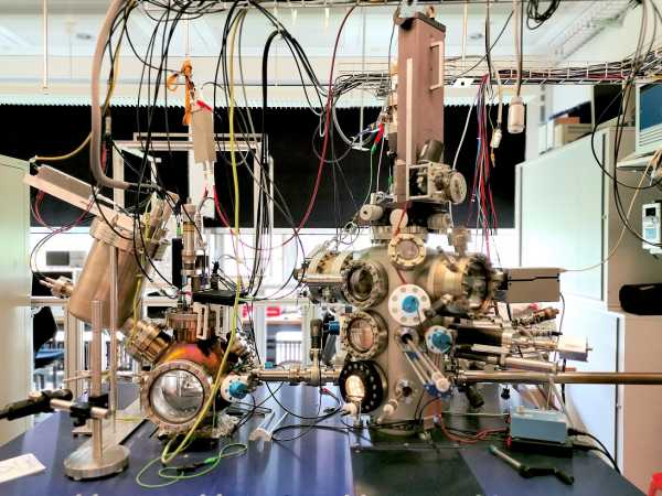
SFEM Setup for Electron Spectro-Microscopy in our laboratory HPT C6.2.
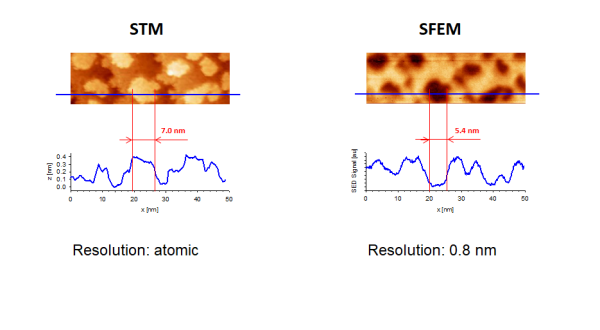
 STM Image (left) and SFEM Image (right) taken from the same region on a W(110) surface covered by 0.34 atomic layers of Fe.
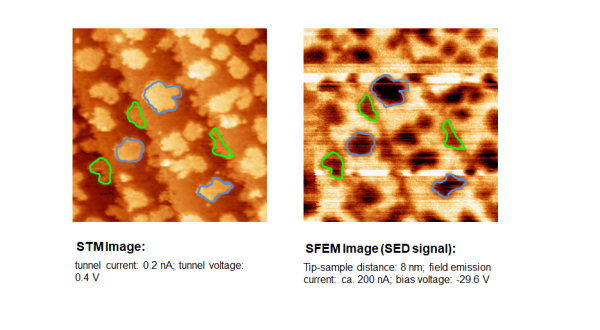 Comparison of the lateral resolution achieved in STM (left) and SFEM (right).
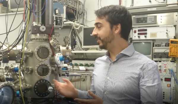
 Our PhD-Student Gabriele Bertolini in front of his preparation chamber.
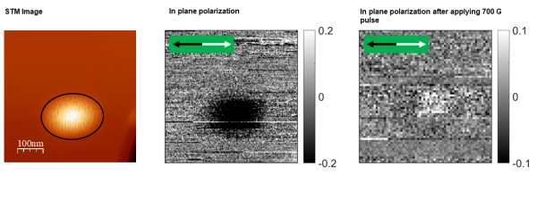
 STM Image (left), in plane polarization (middle) and in plane polarization after applying a 700 G pulse (right), taken on 47 ML Fe on W(110).
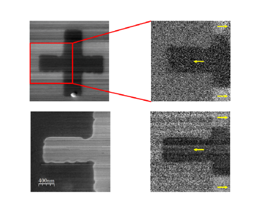
 In Plane magnetization of 47 ML Fe microstructure (cross) on top of W(110); top-left: total electron yield SEMPA, top right: in plane polarization SEMPA, bottom-left: total electron yield SFEMPA, bottom-right: in plane polarization SFEMPA.
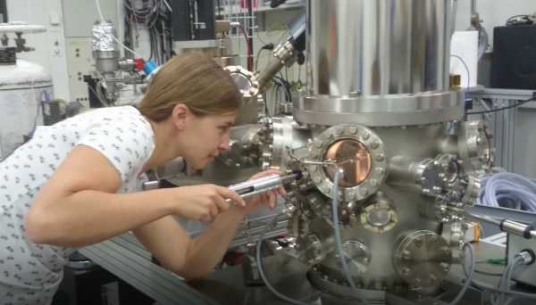
 Our PhD-Student Ann-Katrin Thamm manipulating with a wobble stick in the low temperature SFEM.
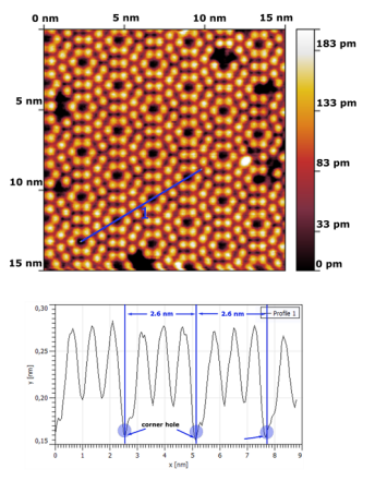
 Atomic resolution with the low-temperature STM at 77 K on a Si 7x7 Sample.

 STM Image (left) and SFEM Image (right) taken from the same region on a W(110) surface covered by 0.34 atomic layers of Fe.
 Comparison of the lateral resolution achieved in STM (left) and SFEM (right).
 Our PhD-Student Gabriele Bertolini in front of his preparation chamber.
 STM Image (left), in plane polarization (middle) and in plane polarization after applying a 700 G pulse (right), taken on 47 ML Fe on W(110).
 In Plane magnetization of 47 ML Fe microstructure (cross) on top of W(110); top-left: total electron yield SEMPA, top right: in plane polarization SEMPA, bottom-left: total electron yield SFEMPA, bottom-right: in plane polarization SFEMPA.
 Our PhD-Student Ann-Katrin Thamm manipulating with a wobble stick in the low temperature SFEM.
 Atomic resolution with the low-temperature STM at 77 K on a Si 7x7 Sample.
